circuit-fantasia > circuit stories > inventing circuits > series resistive losses compensation
I dedicate this story to David Herres from electriciansparadise.com
who appreciates creative thinking...
Inventing Circuits on the Whiteboard...
 How to Compensate Resistive Losses by Series Connected Negative Resistor (Reinventing Negative Impedance Converter)
We have already known what the basic idea behind an odd negative resistor is, how to make negative resistors and how a negative resistor actually works. How, we would like to know where we can apply these exotic elements and what the benefits of these applications are.
In this story, I will show to you one of the most popular negative resistance application - compensating resistive losses. The best way to present this technique is to show the evolution of the initial real voltage source circuit into the final NIC circuit. Following this approach, I will show in eight steps how we can compensate undesired resistive losses by using a series connected current-driven negative resistor. Applying this remedy, first, we will convert an imperfect real voltage source with internal resistance Ri into an almost ideal one. Then, by using a negative resistor, we will compensate also the power losses across a long line having some resistance Rl. Finally, we will compare this technique with the classical negative feedback compensation, in order to show what the advantages and disadvantages of the two approaches are.
As usual, in order to feel how a negative resistor does this magic, we will place ourselves in its place and begin performing its functions. Actually, this is another exciting story about reinventing negative impedance converter (NIC). I hope you have fun. Cyril
Internal links:
1. Starting point: Real voltage source unloaded
2. Problem: Real voltage source loaded
3. Remedy: "Helping" the input voltage source
5. Another problem: Long line resistance
6. Remedy: Increasing the negative resistance
7. Comparing the three sources by visualizing the voltage distribution
8. Negative resistance implementation: NIC
Color key
Links: this page, other my pages, external, multimedia, handmade.
Text: analogies, conclusions.
top < prev step - 1 - 2 - 3 - 4 - 5 - 6 - 7 - 8 - 9 - next step > end
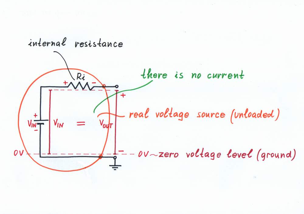
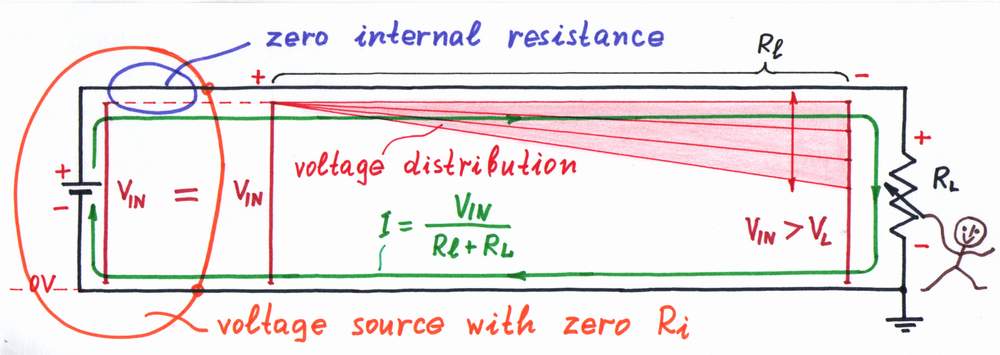
A real voltage source has a voltage VIN and an internal resistance Ri. In the beginning, imagine that there is no load connected (or, the load has an infinite resistance e.g. a digital VOM). So, there is no current flowing through the circuit and there is no voltage drop across the internal resistance Ri. As a result, the output voltage VOUT is equal to the input voltage VIN. We may conclude that actually the imperfect real voltage source placed at ideal no-load conditions acts as an ideal voltage source (VOUT = VIN).
An imperfect real voltage source placed at ideal no-load conditions acts as an ideal voltage source.
Indeed, it sounds strange but yet it is true: the internal resistance Ri is not a resistance as there is no current passing through it. In other words, there is resistance, if there is something to resist:)
In confirmation of this phenomenon, we can see in many cases of our routine that something bad is really bad, if there is an opportunity to evince its/his/her wickedness. Water analogy: the water pressure along the capped pipe is the same no matter of the faucet position (of course, excepting the completely closed position:).
Starting point: Real voltage source unloaded
top < prev step - 1 - 2 - 3 - 4 - 5 - 6 - 7 - 8 - 9 - next step > end
In nature, power sources are limited. So, if we load something (a being, a device etc.) operated by a real power source, it/he/she droops. Mechanical analogy: if we (over)load a car, it decreases its rate of movement. Water analogy: if we open the faucet, the water pressure falls. Human analogy: if something (over)loads us, we droop:)
Problem. Similarly, in electronics, we usually deal with real loads having some finite resistance RL. So, a current I = VIN/(Ri + RL) flows through the circuit and a voltage drop VRi = I.Ri appears across the internal resistor Ri when we load the real input voltage source. From another viewpoint, the internal resistor and the load constitute a voltage divider with ratio K = RL/(Ri + RL); as a result, the output voltage VOUT drops (VOUT = VIN - VRi). What do we do, in order to solve the problem?
Classic solution. Of course, we may connect a voltage follower before the load, in order to decrease the current I (to increase the load resistance). But what will we do in a case of a remote load when the line resistance will evince? Or, imagine that we have an access only to the one (the active) wire...
Suggestion. Remember we had the same problem when we were reinventing the transimpedance amplifier. Then, we used a powerful idea (removing a voltage by an "antivoltage"). Can we apply this trick here? Let's try.
Problem: Real voltage source loaded
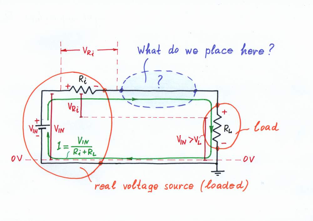
If we load a real voltage source having internal resistance, it droops.
top < prev step - 1 - 2 - 3 - 4 - 5 - 6 - 7 - 8 - 9 - next step > end
Remedy. What can we do in real life when something (operated by a real power source) droops? We can just help it. For this purpose, we usually use an additional power source, which "helps" the main source by compensating only the local losses. Sunny analogy: if there are clouds in the sky or the windows are dirty and we are lazy enough to clean them:), we switch on additional lamps inside the room to "help" the sun.
Implementation. Let's now put this powerful idea into practice. Following it, we have to add so much voltage VH = Ri.I to the input voltage VIN, as much as it loses across the internal resistance Ri. For this purpose, we can place an additional supplementary battery BH in series to the resistor Ri and adjust its voltage so that VH = -VRi. As a result, the "harmful" voltage VRi and the resistance Ri disappear; the output voltage VOUT becomes again equal to the input voltage VIN. Excellent! The "helped" real voltage source has become an ideal voltage source with Ri = 0!
What a wonderful trick it is - just add an adjustable battery in series with the imperfect voltage source and make its voltage equal to the voltage drop across the source internal resistor!
Remedy: "Helping" the input voltage source
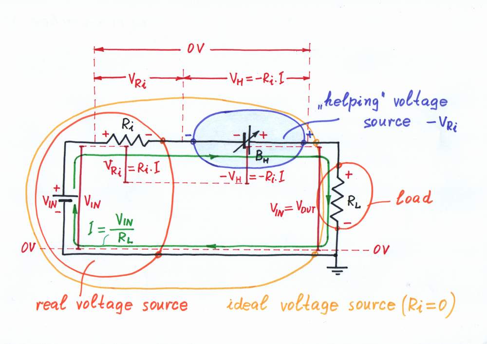
A voltage source with VH = -Ri.I neutralizes the voltage drop VRi = Ri.I.
top < prev step - 1 - 2 - 3 - 4 - 5 - 6 - 7 - 8 - 9 - next step > end
Problem. Only, how do we adjust the compensating voltage VH = -VRi? When we were reinventing the transimpedance amplifier we were observing the voltage drop VRi and were keeping VH equal to it. We were doing that by subtracting the two voltages and observing the result - the virtual ground in point A (i.e., we were applying a negative feedback).
Remedy. Now, we can't apply this technique just because we can't measure the voltage drop VRi (unfortunately, the internal resistance Ri is hidden and distributed inside the source). Well, what can we do then? We can only measure the current flowing through the circuit. Eureka! We have just to restore the voltage drop VRi after the current I and then to measure this "copy" instead the "original"!
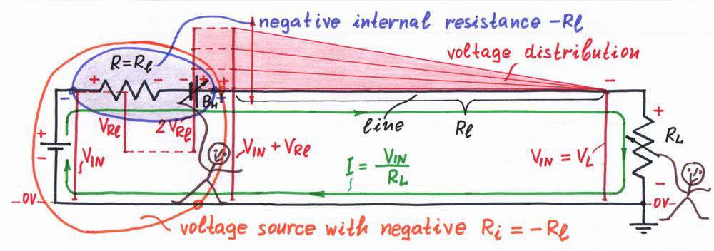
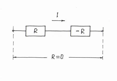
General idea. We can see this powerful idea in our routine when we want to compensate some harmful but inaccessible quantity R. In these cases, we first create a copy of the harmful quantity. Then, we produce two times bigger useful quantity (-2R), in order to compensate both the copy and the original quantity (R + R - 2R = 0).
Implementation. For this purpose, we need an additional current-sensing resistor R = Ri acting as a passive current-to-voltage converter and a "helping" voltage source BH. The "copy" resistor R converts the flowing current I into proportional "mirror" voltage drop VR = R.I = Ri.I = VRi, which drives the compensating voltage source BH. It has first to compensate the "mirror" voltage drop VR; then, to add an additional voltage -VR. So, BH has to act as a "doubling voltage source" producing a voltage VH = -2Ri.I. As a result, the whole circuit will act as a current-controlled voltage source producing a voltage -VR. But this is just a negative resistor! A current-driven negative resistor -Ri "neutralizes" the series connected "positive" one Ri.
Implementation: Making a negative resistor
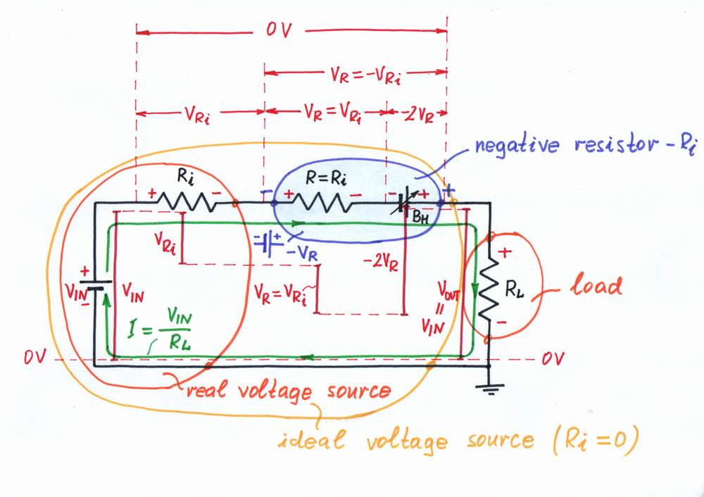
Recipe: In order to compensate a "positive" resistor R, add in series a negative resistor -R.
What do you think? Can we enlarge this powerful idea? For example, can we create in this manner more negative components: a negative capacitor (adding a voltage VC), a negative diode (adding a voltage VF) etc.? I think we can.We have just to use the respective element (a capacitor, a diode etc.) as a "copy" element. But what is the use of doing that? I don't know yet :) Help me!
Current-to-voltage passive converter, Analog electronics 2004: Class 2
top < prev step - 1 - 2 - 3 - 4 - 5 - 6 - 7 - 8 - 9 - next step > end
Compensating the internal "positive" resistance Ri by an external negative resistor -Ri we have managed to assemble an almost ideal voltage source with VOUT = VIN.
Real voltage source + negative resistor = ideal voltage source
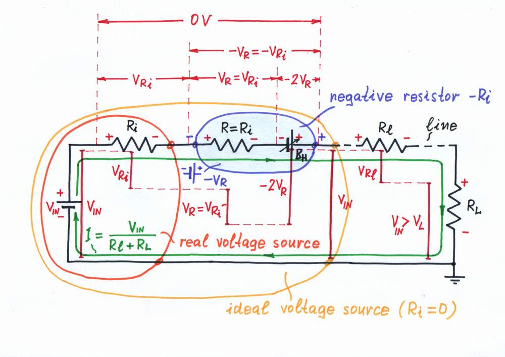
Another problem. Only, a new problem arises when the load stays away, the wire is thin (it has significant resistance) and a big current I flows through the line. This situation is similar to the discussed above - the perfect voltage source that we have created and the line resistance Rl constitute a real voltage source again. As a result, a new harmful voltage drop VRl = I.Rl appears across the line resistance Rl and the output voltage VOUT drops again (VOUT = VIN - VRl).
What do we do, in order to solve the new problem? Maybe, we have to connect in series another negative resistor having resistance VRl:)?
Another problem: Long line resistance
top < prev step - 1 - 2 - 3 - 4 - 5 - 6 - 7 - 8 - 9 - next step > end
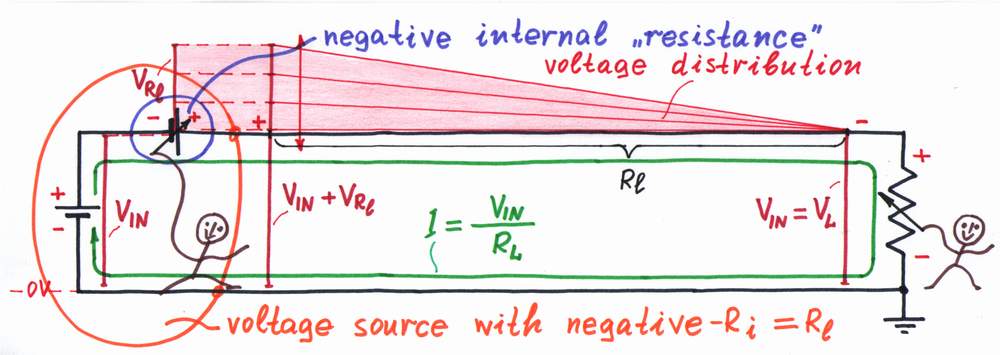
Remedy. Well, I see that you have already guessed:) Of course, we may just increase the negative resistance -R = -(Ri + Rl), in order to compensate both the internal resistance Ri and the line resistance Rl! LEt's do it!
As a result, the doubling voltage source BH begins producing higher "helping" voltage VH = -2(Ri + Rl).I. A portion of this voltage compensates the voltage drop across the "copy" resistor R; the rest part compensates the voltage drops across the internal resistance Ri and the line resistance Rl. As a result, the output voltage becomes again equal to the input voltage VIN.
Note, that the previous ideal voltage source with an internal resistance Ri = 0 "lifts" its output voltage with the value Vl, in order to overcome the line resistance Rl. So, it acts as a voltage source with a negative internal resistance -Rl. The load is supplied by a new ideal voltage source with Rl = 0!
Conclusion. A negative resistor with resistance -R neutralizes R part of the whole series connected "positive" resistance. But what happens, if we go too far trying to compensate the whole of the "positive" circuit resistance (including the load RL) by increasing the "copy" resistance to the value R = Ri + Rl + RL? A suggestion: is there any feedback here? If yes, what kind is it?
Remedy: Increasing the negative resistance
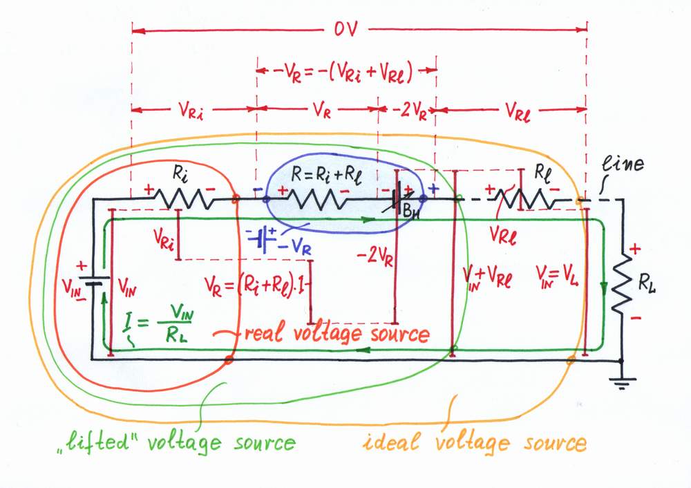
A negative resistor -(Ri + Rl) neutralizes the "positive" resistance (Ri + Rl).
We have already investigated three kinds of voltage sources: a real voltage source with "positive" internal resistance (step 2), an ideal voltage source with zero internal resistance (step 3) and an odd voltage source with negative internal resistance (step 6). Don't you think that it would be interesting to compare their behaviors by investigating the sources at varying load? Well, let's do it.
Making things more attractive. So far, we were visualizing the "external" voltages and voltage drops across the leads of the components (we couldn't "peep" inside the elements). Now, we have the unique (as Ohm, two century ago) opportunity to "feel" the local voltages along the line and then to build the voltage distribution (voltage diagram). In this attractive presentation, each local voltage drop is represented by a local bar with corresponding height. For simplicity, we will draw the envelope of the voltage diagram.
"Inventing" voltage diagram (animated), Voltage diagram (animated), Reproducing the Ohm's experiment
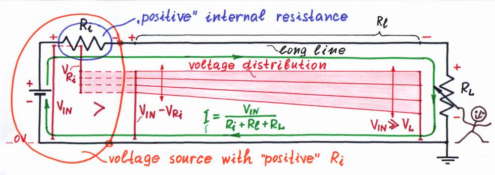
Well, let's begin with the worst case: a real voltage source with internal resistance Ri drives a load through a long line with resistance Rl.
In the beginning, set the load resistance RL too high or just disconnect the load. As we have expected, the output voltage is almost equal to the input voltage (see step 1).
Now, begin decreasing the load resistance RL. A current I flows through the loop. The internal voltage drop VRi increases and the real voltage source droops. In addition, the voltage drop VRl across the line increases; the local voltages along the line decrease gradually from left to right. As a result, the output voltage goes down considerably: VOUT = VIN - VRi - VRl.
A voltage source with "positive" internal resistance
After, let's investigate the better situation: an ideal voltage source with zero internal resistance drives the load through the long line with resistance Rl.
Now, there isn't voltage drop inside the voltage source. So, when we decrease the load resistance RL only the voltage drop VRl across the line increases. As above, the local voltages along the line decrease gradually from left to right. But now, only the right end of the voltage diagram moves vertically; the left end is fixed at VIN level. As a result, the output voltage decreases moderately: VOUT = VIN - VRl.
Note that the ideal voltage source "looks" only after its own output voltage; it is not "interested" in keeping the voltage across the load VRL = VIN.
A voltage source with zero internal resistance
Now, let's scrutinize the most interesting situation: a voltage source with negative internal resistance -Rl drives the load through the long line with resistance Rl.
Wow! What does the voltage source do when we decrease the load resistance RL? Look, it raises the left end of the voltage diagram so much that the right end stays fixed at VIN level! The voltage source does this magic by increasing its voltage with the value VRl - so much as it losses along the long line. As a result, the output voltage remains equal to the input voltage: VOUT = VIN + VRl - VRl = VIN.
It is wonderful trick, isn't it?
A voltage source with negative internal resistance
Finally, don't you think that it is interesting to peep inside the voltage source with negative resistance? Let's do it then!
The "copy" resistor R converts the flowing current I into proportional "mirror" voltage drop VRl = Rl.I, which drives the compensating voltage source BH (an amplifier with K = 2). As a result, the doubling voltage source BH produces an additional "helping" voltage BH = -2.Rl.I. A portion of this voltage compensates the voltage drop across the "copy" resistor R; the rest part compensates the voltage drops across the line resistance Rl. As a result, the voltage source with negative internal resistance raises its output voltage so that the load voltage VL stays equal to the input voltage (VOUT = VIN).
Peeping inside the voltage source with negative internal resistance
top < prev step - 1 - 2 - 3 - 4 - 5 - 6 - 7 - 8 - 9 - next step > end
Building the circuit
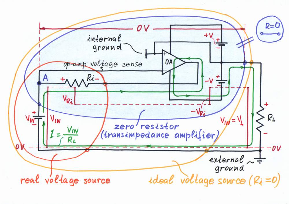
It's time to assemble a real practical circuit with negative resistance, which compensates the resistive losses inside the circuit. Let's for example realize an op-amp version of an ideal voltage source with zero internal resistance by following the basic electrical circuit (step 4). Here is the building "scenario".
First, we have to connect in series with the "original" internal resistor Ri a "copy" element producing a "mirror" voltage drop VRi. Of course, it will be a "positive" resistor with the same resistance R = Ri.
Then, we have to include in series with the "copy" resistor R a "helping" voltage source. For this purpose, we may use the output part of a properly supplied op-amp OA. For clarity, the circuit is "flying"; it has an internal ground, which is the middle point of the split power supply.
Finally, we have to make the op-amp produce two times higher output voltage VOA than the "mirror" voltage drop VR = VRi across the "copy" resistor R. The op-amp will do this "magic", if we make it compare 1/2 of its output voltage VOA with the "mirror" voltage drop VR = VRi across the "copy" resistor R. Aha, a voltage divider consisting of two equal resistors R and connected between the output and the non-inverting intput will work fine!
Negative resistance implementation: NIC
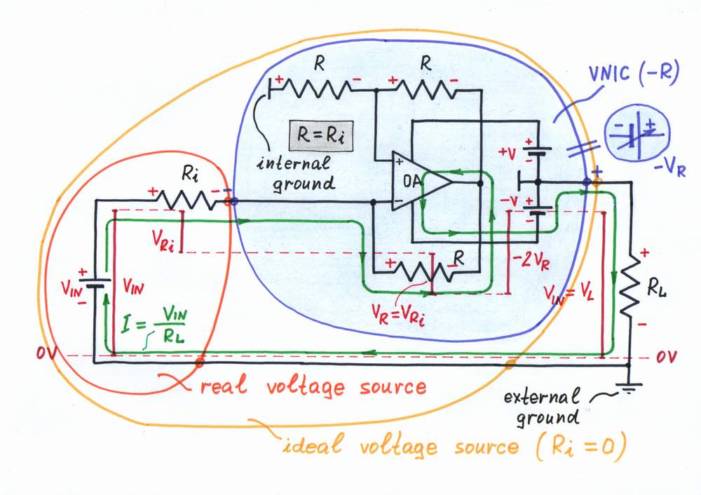
In an NIC, the op-amp acts just as a small battery, which adds so much voltage as it loses across the resistor Ri.
Circuit operation
When we apply a positive input voltage VIN a current IIN begins flowing through the circuit in direction VIN > Ri > R > op-amp output > RL. As a result, a voltage drop VR appears across the lower resistor R and the load RL. If the op-amp is slow enough, it does not react at the first moment. Its output voltageVOA remains zero (toward the internal ground) and a positive voltage V(-) = (R + RL)/(Ri + R + RL) appears (toward the external ground) at the inverting input. The op-amp "notes" that and reacts: it begins decreasing its output voltage by sucking the current IIN and continously comparing the voltage drops across the two resistors R connected between the output and the two inputs.
The op-amp stops when it manages to zero the voltage difference between its inputs (0.5VOA - VRi = 0).At this moment, the output voltage is exactly as much as needed (VOA = 2VRi). The voltage is connected in one and the same direction (- VIN +, - VOA +) with the input voltage VIN, so that the two voltages are added.
Question. Maybe, you have noted that there are two feedbacks (negative and positive) in this odd circuit. What do you think? Can this connection cause a problem with the stability?
Answer. The positive feedback returns a voltage V(+) = R/(R + R) = 0.5VOA to the non-inverting input; the negative feedback returns higher voltage V(-) = (Ri + RL)/(Ri + RL + R) to the inverting input. As a result, the negative feedback dominates; the circuit is stable.
top < prev step - 1 - 2 - 3 - 4 - 5 - 6 - 7 - 8 - 9 - next step > end
But we have already solved the same problem (compensating resistive losses) when we were reinventing the famous circuit of a transimpedance amplifier! Then, what is the difference between the two circuits? What circuit is better?
Transimpedance amplifier. The op-amp of a transimpedance amplifier compares its output voltage directly with the "original" voltage drop across the "harmful" resistance. In this way, it will compensate exactly the resistance even when it varies (e.g., because of temperature or length variations). Only, for this purpose the op-amp needs an additional voltage sense wire, in order to "observe" the virtual ground in point A by its inverting input. Unfortunately, in many cases (as in our case above), this point is just inaccessible!
A transimpedance amplifier consumes power only of PTA = VRi.I.
Negative resistor. The op-amp of an NIC compares its output voltage with a "mirror" voltage drop across a "copy" resistance instead with the "original" resistance (it "supposes" that the two resistances are equal). But what happens, if the "original" resistance varies? The op-amp will be misled and an error will appear. Only, a negative resistor has an advantage - it has only two terminals; so, it needs only two wires (it is a 1-port amplifier).
An NIC consumes two time more power (PNIC = 2VRi.I = 2PTA) than a transimpedance amplifier since it has to compensate two voltage drops VRi.
Comparison with the negative feedback implementation
A transimpedance amplifier is another circuit, which can compensate resistive losses by means of negative feedback. It is precise and economical circuit; only, it needs an additional voltage sense wire.
top < prev step - 1 - 2 - 3 - 4 - 5 - 6 - 7 - 8 - 9 - 10 - next step > end
Warning: this is only a humor! Don't you think that all these explanations, analogies, voltage bars and diagrams, current loops etc. are unnecessary:)? Instead, especially if we are teachers who don't like to waste our time in explaining circuit phenomena to students (I know such teachers), we can just say, "Connect in series with the positive resistor R a negative resistor -R, in order to get zero resistance (R - R = 0)."
How simple and clear it sounds! How convenient for lecturers it is! But how nonundestandable for students it is! Even, if we back up this formal speculation with all kinds of formulas, it will remain nonunderstandable because the basic idea of the phenomenon is hidden!
I hope you don't do that! If you think so, I will be glad to get in touch with you.
Formal explanation (if we only were bad teachers...)
Last updated April 7, 2007